Key points
- The technique uses the spin Hall effect of light to convert atomic-layer thickness into features seen at a material's edges.
- In one regime, the orientation of edge features changes continuously as the number of layers changes.
- In another regime, a feature switching from disk to ring gives a discrete marker of layer number.
- The team demonstrated layer-resolved imaging in graphene, MoS2 and WSe2.
Researchers have developed an optical imaging method that shows how many atomic layers make up a sheet of two-dimensional material. It works by turning that thickness into patterns you can see along the sheet's edges. The team reports the work in Nature Communications and demonstrates it on graphene, MoS2 and WSe2.
Counting layers matters because materials only a few atoms thick behave differently depending on how many layers they have. According to the authors, the usual tools rely on spectroscopic signatures or scanning probes. These need complex equipment and often produce results that are hard to read directly as an image.
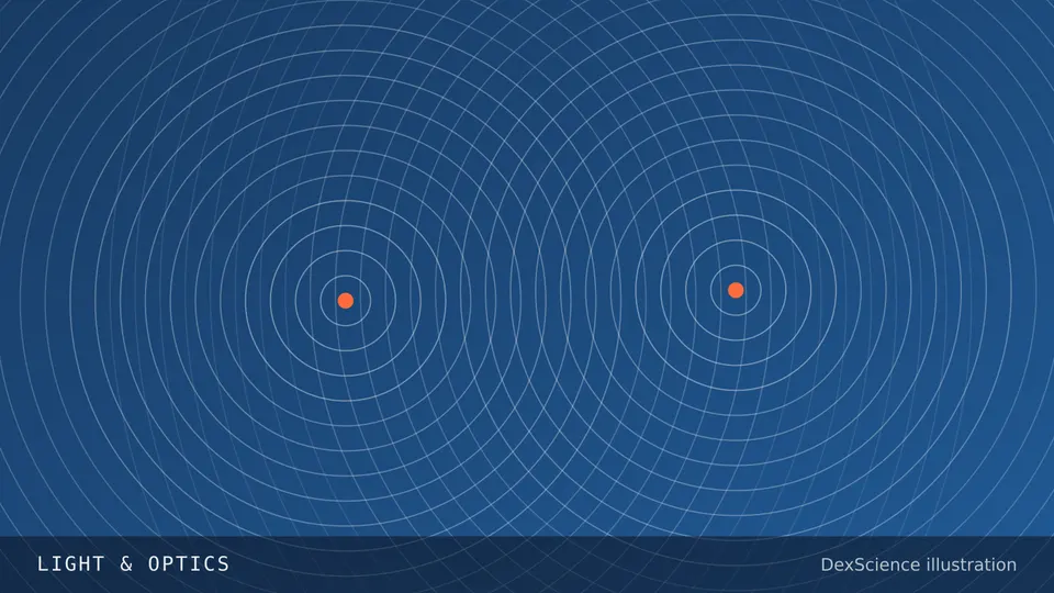
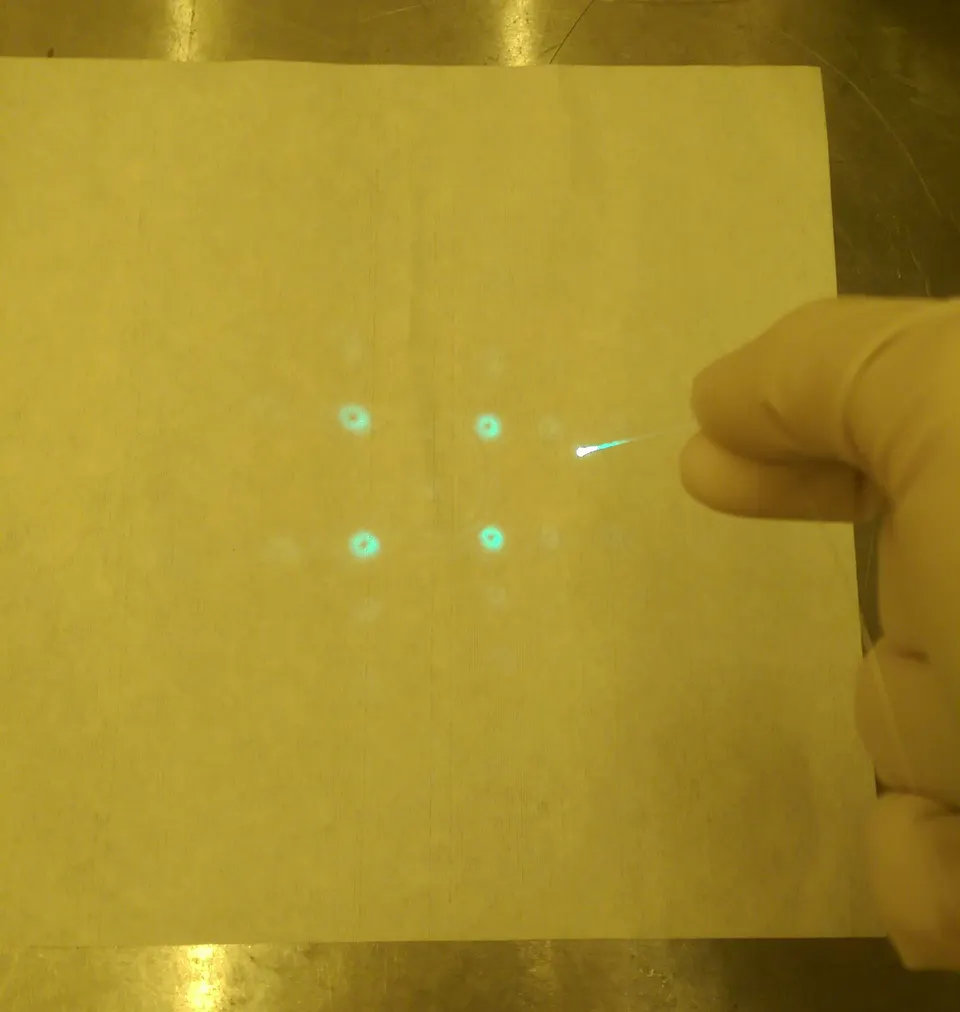
The new approach relies on the spin Hall effect of light, in which light of opposite circular polarization is pushed slightly apart as it reflects or refracts at an interface. The researchers tuned how flat interfaces pass along light, which gave them access to two imaging modes. In the anisotropic mode, the direction of the edge features shifts smoothly as the layer number changes. In the isotropic mode, a feature changes shape from a disk to a ring. That switch, the researchers say, offers a robust, step-like signal for identifying layers.
The authors describe the method as simple and versatile, and say it could allow rapid, in situ characterization of two-dimensional materials. The paper is a peer-reviewed, accepted version that the journal released early. It may still be edited before the final version is published.
Why it matters
Because the properties of two-dimensional materials depend on how many layers they have, a simple optical way to read thickness could make it faster to characterize these materials, the authors say.
What we don't know yet
The article is an early, accepted version that may still change before the final Version of Record. The source summary also does not say how well the method performs beyond the three materials tested.
Terms in this story
- Two-dimensional material
- A crystal only one or a few atomic layers thick, such as graphene.
- Spin Hall effect of light
- A small sideways separation of light with opposite circular polarization when it meets an interface.
- In situ
- Measured in place, without moving the sample to a separate instrument.
Sources and verification
DexScience articles are produced with AI assistance and an automated fact-check against the linked sources. Spotted an error? Tell us and we will correct it openly.